On the lithography floor, soft bake is not some warm-up lap. It’s the step that sets the photoresist solvent profile, locks in film thickness, and writes the dimensional tolerances that carry straight into exposure and development. When the bake is uneven, you don’t get a gentle drift. You get line-width variation, sidewall footing, and a yield hit that shows up right where it hurts—parametric test. Conventional hotplates can hide non-uniformity with long soak times, but wafers keep changing. Pattern density shifts, stack heights vary, and substrates keep getting thinner—each one moves the thermal load. Infrared heating, when it’s built for semiconductor discipline, pulls that mask off. It delivers heat where it needs to go—fast, and with repeatable control.
What matters: IR precision, measured in wafer results
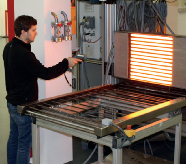
Soft bake is fundamentally a thermal budget problem. The resist has to hit target temperature quickly enough to drive off solvent, but not so long that the polymer starts to change before exposure. IR shortens the path from setpoint to stabilization—if the irradiance field is uniform and controllable. We match short-wave infrared emitters to the absorption behavior of common resist stacks. That gives sub-millimeter spatial control over the heated zone, which translates into tight temperature uniformity across the wafer surface. In practice, you can hold wafer-level uniformity within tight tolerances—typically ±0.1°C across the bake surface—without leaning on the mechanical flattening of a thick platen. Repeatability is just as important as uniformity. Every bake cycle has to look the same, shift after shift. The system uses closed-loop control with calibrated sensors and an emitter array that minimizes edge fall-off. The algorithm doesn’t chase an average temperature; it manages the spatial profile so the center and edge get the same effective thermal dose. That’s why IR fits soft bake so well: the response is fast, the thermal mass is low, and the energy can be shaped. For photoresist, that means consistent solvent removal, predictable film thickness, and a stable baseline for the exposure latitude advanced nodes demand.
Why it works in production: soft bake, done right—every time
In a production lithography cell, the soft bake station is under constant pressure. Throughput wants shorter bake times. Yield wants tight distributions. And the cleanroom wants equipment that doesn’t turn into a particle source. IR-based soft bake cuts the bake window without giving up control. The resist hits setpoint fast, and the shorter thermal exposure reduces unwanted flow and chemistry changes. That feeds directly into tighter CD control and lower defectivity. The platform is built for cleanroom reality. Components are chosen to minimize outgassing, and the heating chamber is shaped to avoid air turbulence that stirs up particles. In Class 1–100 environments, particle generation stays near zero—so you don’t have to trade thermal performance for contamination control. Reliability shows up as uptime. Emitter life is long—multiple thousands of hours—and the architecture supports 24/7 operation with predictable maintenance windows. When the bake is repeatable, the rest of the lithography stack settles down: exposure doses stay consistent, development times don’t drift, and the rework queue shrinks. You also pick up real operational gains. Energy use drops because IR heats the wafer and resist directly instead of heating a large platen and waiting on equilibrium. Lower thermal mass means less power during warm-up and idle. Maintenance intervals stretch because there’s no large heated plate to degrade, and the control loop is simpler and more direct.
The practical details: integration, compatibility, and one honest constraint
IR soft bake isn’t a plug-and-play swap for every hotplate setup. Integration is straightforward, but you need to pay attention in three places: thermal interface, cleanroom interface, and control interface. The thermal interface has to match your wafer size and cassette handling. The chamber needs to accept your standard carriers and keep the right spacing for uniform irradiance. The control interface has to line up with your SECS/GEM communication and recipe management. We can integrate into existing lithography tracks and stand-alone bake stations, but the installation plan has to include footprint, utilities, and the software handshake. Material compatibility is another real-world consideration. IR absorption depends on the stack. For standard photoresist and common bottom anti-reflective coatings, the absorption match is strong and the process window is wide. For highly reflective or unusual stacks, you may need a quick qualification run to tune setpoint and irradiance profile—so you clear solvent without driving skin effects. That’s not a flaw in IR; it’s normal when you change films. And here’s the one constraint worth stating plainly: infrared heating is line-of-sight. Edge-bead geometry and local topography can scatter the field, and that can affect the very edge of the wafer. In most production recipes, you handle this with a controlled edge exclusion and by tuning the irradiance map. If your process truly requires baking right to the edge with no exclusion, you need to talk through the edge-mapping strategy during qualification. On the lithography floor, repeatability starts at soft bake. IR gives you sub-millimeter control of the thermal field, tight uniformity, and a process signature you can bank on shift after shift. That’s how you keep photoresist in spec, cut variation, and keep yield on plan.