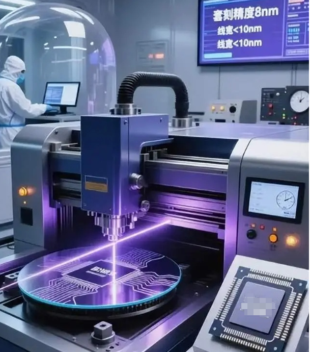
Out on the line, Mini LED chips don’t tolerate thermal drift. If the packaging lamp swings more than ±0.1°C, you’re looking at shifted eutectic bonds, color coordinates that drift, and yield that falls off a cliff. We built this lamp for the fab floor, not a marketing deck. What matters, technically: The lamp holds ±0.1°C uniformity across the zone, with multi-zone closed-loop control that keeps the thermal budget tight. It plays nice in cleanrooms Class 1–100—sealed quartz and ceramic assemblies, materials that don’t outgas, and a laminar flow path that keeps particle generation down to single-digit counts per cubic foot. Photoresist bake profiles—soft bake and hard bake—track within ±0.5% repeatability, so linewidth and sidewall profiles stay in spec lot after lot. Why this works in Mini LED packaging: The lamp drives reflow, epoxy cure, and interconnect formation. Tight thermal control means less rework, consistent binning, and faster changeovers. Clean compatibility lets you run it right inside lithography and packaging cells without stacking on extra particle mitigation. Energy use drops thanks to efficient IR emitters and smart duty cycling, and MTBF pushes into tens of thousands of hours—fewer surprises, less unplanned downtime. Here are the practical details: Installation needs a dedicated 24 VDC control line and a clean air supply matched to the lamp’s exhaust. The unit fits standard packaging platforms, but you still have to qualify the thermal profile for each substrate stack and adhesive. There’s a short ramp-up while you lock the process window. Once you do, the system settles into process-room repeatability.